- 您现在的位置:买卖IC网 > Sheet目录2098 > MK2069-01GILFTR (IDT, Integrated Device Technology Inc)IC VCXO CLK SYNCHRONIZER 56TSSOP
MK2069-01
VCXO-BASED LINE CARD CLOCK SYNCHRONIZER
VCXO AND SYNTHESIZER
IDT VCXO-BASED LINE CARD CLOCK SYNCHRONIZER
19
MK2069-01
REV K 051310
Note 1: This is the recommended crystal operating range. A crystal as low as 8 MHz can be used, although this may
result in increased output phase noise.
Note 2: The VCXO crystal will be pulled to its minimum frequency when there is no input clock (CLR = 1) due to the
attempt of the PLL to lock to 0 Hz.
Note 3: The minimum practical input frequency is 1 kHz. Through proper loop filter design lower input frequencies
may be possible.
Note 4: The output of RCLK is a positive pulse with a duration equal to VCLK high time, or half the VCLK period.
Note 5: Referenced to ICLK, the skews of VCLK, RCLK and TCLK increase together when leakage is present in the
external VCXO PLL loop filter.
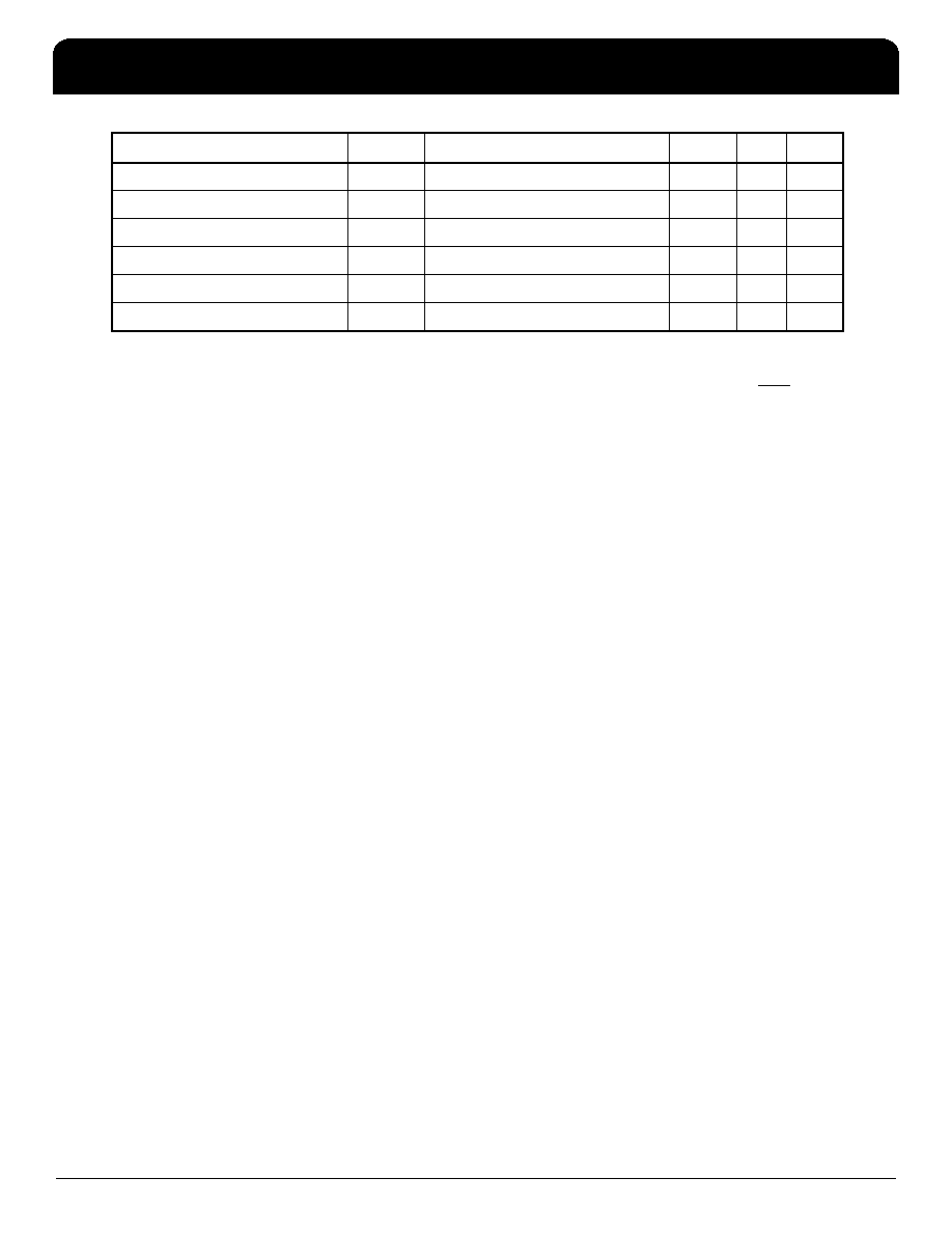
Output Rise Time, TCLK
tOR
0.8 to 2.0V, CL=15pF
0.75
1
ns
Output Fall Time, TCLK
tOF
2.0 to 0.8V, CL=15pF
0.75
1
ns
Skew, ICLK to VCLK (Note 5)
tIV
Rising edges, CL=15pF
-5
2.5
+10
ns
Skew, ICLK to RCLK (Note 5)
tIV
Rising edges, CL=15pF
+5
10
+20
ns
Skew, ICLK to TCLK (Note 5)
tVT
Rising edges, CL=15pF
-5
1.5
+10
ns
Nominal Output Impedance
ZOUT
20
Ω
Parameter
Symbol
Conditions
Min.
Typ.
Max. Units
发布紧急采购,3分钟左右您将得到回复。
相关PDF资料
MK2069-04GILFTR
IC VCXO CLK TRANSLATOR 56-TSSOP
MK2302S-01LFTR
IC MULTIPLIER/ZD BUFFER 8-SOIC
MK2304S-2LF
IC PLL ZD BUFFER LO SKEW 8-SOIC
MK2703SILF
IC PLL AUD CLK SYNTHESIZER 8SOIC
MK2704SLF
IC PLL AUD CLK SYNTHESIZER 8SOIC
MK2716SLFTR
IC CLK SYNTHESIZER HDTV 8-SOIC
MK2732-06GLF
IC VCXO/MULTIPLIER 16-TSSOP
MK2745-21SLFTR
IC CLK SOURCE DVD/MPEG 16-SOIC
相关代理商/技术参数
MK2069-01GITR
功能描述:IC VCXO CLK SYNCHRONIZER 56TSSOP RoHS:否 类别:集成电路 (IC) >> 时钟/计时 - 时钟发生器,PLL,频率合成器 系列:- 标准包装:39 系列:- 类型:* PLL:带旁路 输入:时钟 输出:时钟 电路数:1 比率 - 输入:输出:1:10 差分 - 输入:输出:是/是 频率 - 最大:170MHz 除法器/乘法器:无/无 电源电压:2.375 V ~ 3.465 V 工作温度:0°C ~ 70°C 安装类型:* 封装/外壳:* 供应商设备封装:* 包装:*
MK2069-03
制造商:ICS 制造商全称:ICS 功能描述:VCXO-Based Clock Translator with High Multiplication
MK2069-03GI
功能描述:IC VCXO CLK TRANSLATOR 56-TSSOP RoHS:否 类别:集成电路 (IC) >> 时钟/计时 - 时钟发生器,PLL,频率合成器 系列:- 标准包装:27 系列:Precision Edge® 类型:频率合成器 PLL:是 输入:PECL,晶体 输出:PECL 电路数:1 比率 - 输入:输出:1:1 差分 - 输入:输出:无/是 频率 - 最大:800MHz 除法器/乘法器:是/无 电源电压:3.135 V ~ 5.25 V 工作温度:0°C ~ 85°C 安装类型:表面贴装 封装/外壳:28-SOIC(0.295",7.50mm 宽) 供应商设备封装:28-SOIC 包装:管件
MK2069-03GITR
功能描述:时钟发生器及支持产品 VCXO-BASED CLOCK TRANSLATOR RoHS:否 制造商:Silicon Labs 类型:Clock Generators 最大输入频率:14.318 MHz 最大输出频率:166 MHz 输出端数量:16 占空比 - 最大:55 % 工作电源电压:3.3 V 工作电源电流:1 mA 最大工作温度:+ 85 C 安装风格:SMD/SMT 封装 / 箱体:QFN-56
MK2069-04
制造商:ICS 制造商全称:ICS 功能描述:VCXO-Based Universal Clock Translator
MK2069-04GI
功能描述:IC VCXO CLK TRANSLATOR 56-TSSOP RoHS:否 类别:集成电路 (IC) >> 时钟/计时 - 时钟发生器,PLL,频率合成器 系列:- 标准包装:39 系列:- 类型:* PLL:带旁路 输入:时钟 输出:时钟 电路数:1 比率 - 输入:输出:1:10 差分 - 输入:输出:是/是 频率 - 最大:170MHz 除法器/乘法器:无/无 电源电压:2.375 V ~ 3.465 V 工作温度:0°C ~ 70°C 安装类型:* 封装/外壳:* 供应商设备封装:* 包装:*
MK2069-04GILF
功能描述:时钟发生器及支持产品 VCXO-BASED UNIVERSAL CLOCK TRANSLATOR RoHS:否 制造商:Silicon Labs 类型:Clock Generators 最大输入频率:14.318 MHz 最大输出频率:166 MHz 输出端数量:16 占空比 - 最大:55 % 工作电源电压:3.3 V 工作电源电流:1 mA 最大工作温度:+ 85 C 安装风格:SMD/SMT 封装 / 箱体:QFN-56
MK2069-04GILFTR
功能描述:时钟发生器及支持产品 VCXO-BASED UNIVERSAL CLOCK TRANSLATOR RoHS:否 制造商:Silicon Labs 类型:Clock Generators 最大输入频率:14.318 MHz 最大输出频率:166 MHz 输出端数量:16 占空比 - 最大:55 % 工作电源电压:3.3 V 工作电源电流:1 mA 最大工作温度:+ 85 C 安装风格:SMD/SMT 封装 / 箱体:QFN-56